ADT6401/ADT6402
Data Sheet
Rev. C | Page 4 of 12
ABSOLUTE MAXIMUM RATINGS
Table 2.
Parameter
Rating
VCC to GND
0.3 V to +7 V
S0, S1, S2 Input Voltage to GND
0.3 V to VCC + 0.3 V
Open-Drain Output Voltage to GND
0.3 V to +7 V
Push-Pull Output Voltage to GND
0.3 V to V
CC
+ 0.3 V
Input Current on All Pins
20 mA
Output Current on All Pins
20 mA
ESD rating (HBM)
1.5 kV
Operating Temperature Range
55癈 to +125癈
Storage Temperature Range
65癈 to +160癈
Maximum Junction Temperature, T
JMAX
150.7癈
6-Lead SOT-23 (RJ-6)
Power Dissipation
1
WMAX = (TJMAX TA
2
)/?SPAN class="pst ADT6402SRJZ-RL7_2322505_5">JA
Thermal Impedance
3
?/DIV>
JA
, Junction-to-Ambient (Still Air) 229.6癈/W
IR Reflow Soldering (RoHS-Compliant
Package)
Peak Temperature
260癈 (+0癈)
Time at Peak Temperature
20 sec to 40 sec
Ramp-Up Rate
3癈/sec maximum
Ramp-Down Rate
6癈/sec maximum
Time 25癈 to Peak Temperature
8 minute maximum
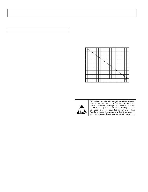
1
Values relate to package being used on a standard 2-layer PCB, which gives a
worst-case ?SPAN class="pst ADT6402SRJZ-RL7_2322505_6">JA. Refer to Figure 2 for a plot of maximum power dissipation vs.
ambient temperature (TA).
2
T
A
= ambient temperature.
3
Junction-to-case resistance is applicable to components featuring a
preferential flow direction, for example, components mounted on a
heat sink. Junction-to-ambient resistance is more useful for air-cooled,
PCB-mounted components.
Stresses above those listed under Absolute Maximum Ratings
may cause permanent damage to the device. This is a stress
rating only; functional operation of the device at these or any
other conditions above those indicated in the operational
section of this specification is not implied. Exposure to absolute
maximum rating conditions for extended periods may affect
device reliability.
0.9
0
125
TEMPERATURE 癈
0.8
0.7
0.6
0.5
0.4
0.3
0.2
0.1
55
50
40
30
20
10
0
10
20
30
40
50
60
70
80
90
100
110
120
SOT-23 PD @ 125癈 = 0.107W
Figure 2. SOT-23 Maximum Power Dissipation vs. Temperature
ESD CAUTION
发布紧急采购,3分钟左右您将得到回复。
相关PDF资料
ADT6501SRJZP085RL7
IC TEMP SENSOR MICROPWR SOT23-5
ADT7302ARTZ-500RL7
IC SENSOR TEMP 13BIT DGT SOT23-6
ADT7310TRZ
IC TEMP SENSOR 16BIT SPI 8SOIC
ADT7461AARMZ-R
IC TEMP SENSOR DGTL 2CH 8-MSOP
ADT7461ARMZ-2R
IC TEMP SENSOR DGTL 2CH 8-MSOP
ADT7463ARQZ-REEL
IC REMOTE THERMAL CTRLR 24-QSOP
ADT7476AARQZ-R
IC REMOTE THERMAL CTLR 24QSOP
ADT7481ARMZ-1RL
IC SENSOR TEMP 2CH ALARM 10MSOP
相关代理商/技术参数
ADT6501
制造商:AD 制造商全称:Analog Devices 功能描述:Low Cost, 2.7 V to 5.5 V, Micropower Temperature Switches in SOT-23
ADT6501ARJP035
制造商:AD 制造商全称:Analog Devices 功能描述:Low Cost, 2.7 V to 5.5 V, Micropower Temperature Switches in SOT-23
ADT6501ARJP045
制造商:AD 制造商全称:Analog Devices 功能描述:Low Cost, 2.7 V to 5.5 V, Micropower Temperature Switches in SOT-23
ADT6501ARJP055
制造商:AD 制造商全称:Analog Devices 功能描述:Low Cost, 2.7 V to 5.5 V, Micropower Temperature Switches in SOT-23
ADT6501ARJP065
制造商:AD 制造商全称:Analog Devices 功能描述:Low Cost, 2.7 V to 5.5 V, Micropower Temperature Switches in SOT-23
ADT6501ARJP075
制造商:AD 制造商全称:Analog Devices 功能描述:Low Cost, 2.7 V to 5.5 V, Micropower Temperature Switches in SOT-23
ADT6501ARJP085
制造商:AD 制造商全称:Analog Devices 功能描述:Low Cost, 2.7 V to 5.5 V, Micropower Temperature Switches in SOT-23
ADT6501ARJP095
制造商:AD 制造商全称:Analog Devices 功能描述:Low Cost, 2.7 V to 5.5 V, Micropower Temperature Switches in SOT-23